Rehan Kapadia
Director MOSIS 2.0
| Foundry Service | Technology Node | Tapeout Date |
|---|---|---|
| TSMC | 22 nm | 9/2/2026 |
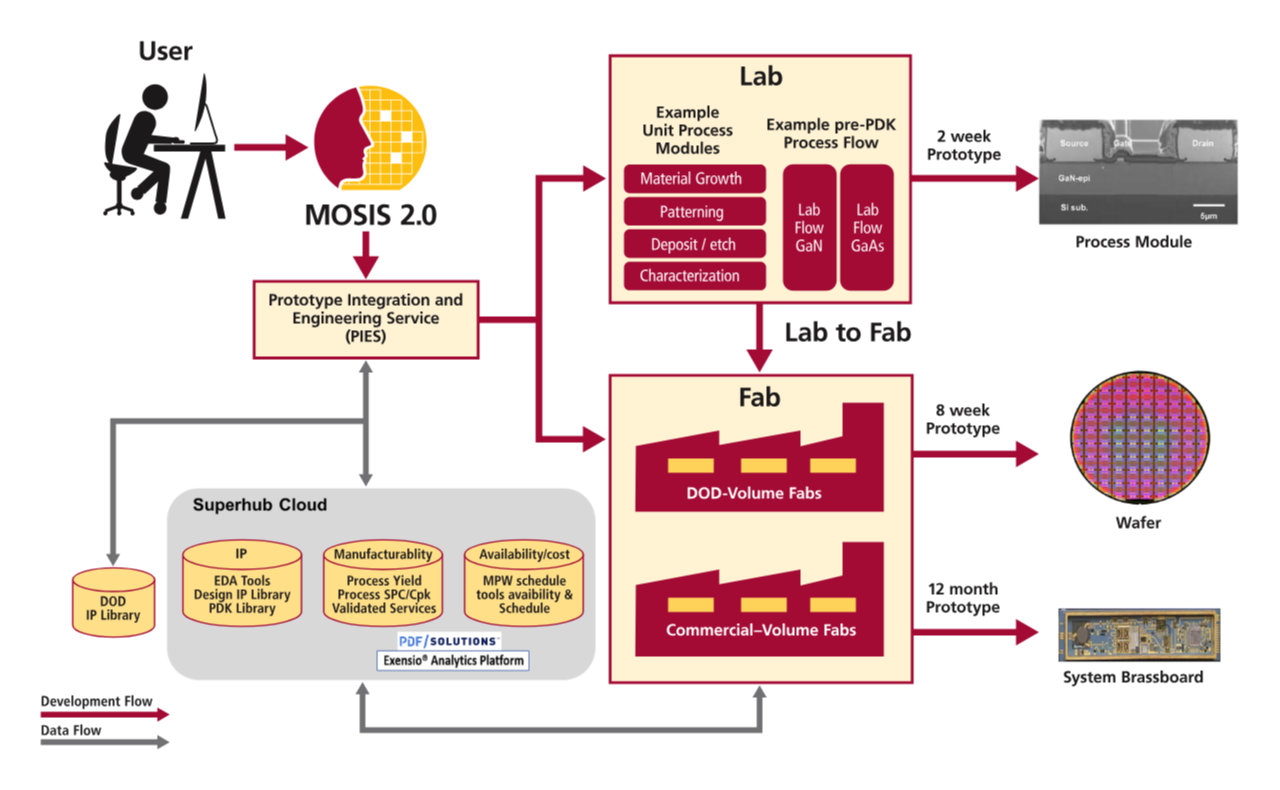
Rapid prototyping and process development capability through access to seven university nanofabrication facilities and other experimental prototyping facilities within the Southern California area and throughout the nation.
Supporting both silicon CMOS and advanced compound semiconductor technologies with seamless access to a wide array of commercial silicon MPW services from leading large, medium, and small-volume foundries.
Providing comprehensive chip design services that simplify and streamline the development process, enabling customers to bring their innovative ideas from concept to silicon.
The SWAP Hub provides a suite of test and modeling services to evaluate materials, devices, packages, and full systems across a wide range of environments for mission-critical applications.
MOSIS 2.0/MMEC Booth 630
Long Beach Convention & Entertainment Center
July 27-29
MOSIS 2.0 is the central storefront and gateway to access cutting-edge prototyping services, targeting advanced RF, 5G/6G, and EW applications.
The Prototype Integration and Engineering Service (PIES) Team is at the core of MOSIS 2.0 - a dedicated fab-knowledgeable engineering group that supports designers to accelerate their innovations to solutions.
We invite innovators, researchers, and industry partners to engage with MOSIS 2.0-and join us in advancing next-generation microelectronics.
Director MOSIS 2.0
Fab Prototyping Services Manager
Senior Project Manager
Microelectronics Fabrication Engineering Manager
Receive notifications for new MOSIS 2.0 offerings and upcoming MPW runs.
If you're attending the conference, visit Booth 630, where you can chat with @[Jeung Hun Park](urn:li:person:nEUQcKuwV_) and the team.
Whether you're exploring semiconductor design, prototyping, or fabrication opportunities, we'd love to discuss how we can help accelerate your next project.
See you at @[DAC, The Chips to Systems Conference](urn:li:organization:6254598)!
If you're attending the @[DAC, The Chips to Systems Conference](urn:li:organization:6254598), be sure to stop by Booth 630 and chat with the MOSIS 2.0 and MMEC teams.
Whether you're looking to accelerate your semiconductor design, prototyping, or fabrication project, we'd love to talk about how our services can help bring your ideas to silicon.
📍 Booth 630 | Long Beach Convention & Entertainment Center
We look forward to meeting you!
Learn how this value-added collaboration is expanding access to world-class semiconductor technologies for the MOSIS 2.0 community. Through the MOSIS 2.0 storefront, customers can now leverage GlobalFoundries' full portfolio of process technologies—including advanced FinFET and FDX™ FD-SOI platforms—to help accelerate innovative chip designs from concept to fabrication.
Read more: https://lnkd.in/gFfgzXuB
The MOSIS 2.0 team will be attending @[DAC, The Chips to Systems Conference](urn:li:organization:6254598) Long Beach, alongside our colleagues from MMEC.
📅 Expo Dates: July 27–29, 2026
📍 Venue: Long Beach Convention & Entertainment Center
🏢 Visit us at Booth 630
Whether you're developing the next generation of semiconductor technologies or looking to bring your next chip design to life, stop by Booth 630 to learn how we can help simplify your path from concept to silicon with fabrication, prototyping, and design enablement services.
If you're planning to attend, register for the free I ❤️ DAC Pass: https://lnkd.in/e-Nmf_5b
If you're attending, be sure to connect with Christine Lee, our Fab Prototyping Services Manager, to learn how MOSIS 2.0 is helping accelerate semiconductor innovation by expanding access to cutting-edge prototyping services.
Find out more about the event: https://lnkd.in/gzkht9yT
Business Council for International Understanding (BCIU)