Nanofab Prototyping
MOSIS 2.0 offers rapid prototyping and process development capability through access to seven university nanofabrication facilities (USC, UCI, UCLA, UCR, UCSB, UCSD, and Caltech) and three DoW-volume fabs (Northrop Grumman, Teledyne, and HRL Laboratories) within the Southern California area. Our university and industry partners have extensive process experience in silicon CMOS and advanced compound semiconductor technologies (GaAs, InP, GaN HEMT/HBT) and can support development on wafer sizes from 100mm to 300mm. The MOSIS 2.0 Prototype Integration and Engineering Service (PIES) team also provides white-glove process development service to enable customer needs to be seamlessly translated to quality prototypes/products via process flow development, fabrication oversight, and quality and test controls implemented at each critical process step.
Our Nanofabrication Partners
Available Fab Capability
Process Categories
| Lithography | PVD | CVD | Dry Etch | Wet Process | Thermal |
|---|---|---|---|---|---|
| Aligner, Contact Aligner, E-beam, FIB, Maskless Aligner, Stepper (i-line, DUV) | E-beam, Sputter (DC/RF), Thermal | PECVD, LPCVD, ALD, Thermal Plasma, Parylene | ICP-RIE, RIE/DRIE, ALE, Plasma Asher, IBE, lon Mill, Vapor Etch (XeF2, HF) | HF/BOE, Metal Etch, KOH, Solvent Clean, Acid Clean, Electroplating | RTP, Tube, Furnace, Oxidation (Dry, Wet), Anneal |
Additional Process Equipment
| CMP | Laser Processing | Surface Mod | Clean |
|---|---|---|---|
| Mechanical Polisher, Lapper, Grinder | UV Excimer Laser, Laser Micro-machining | UV Ozone, MVD | Solvent Bench, Acid Clean, Ultrasonic |
Substrates
| Size (mm) | ||
|---|---|---|
| Type | Mininum | Maximum |
| Silicon | pieces | 200 |
| III-V | pieces | 150 |
| Glass | pieces | 200 |
| Polymer | pieces | 150 |
Process Specifications
| Size (mm) | ||
|---|---|---|
| Process Type | Mininum | Maximum |
| Lithography (Aligner) | pieces | 200 |
| E-Beam | pieces | 200 |
| ALD | pieces | 200 |
| PECVD | pieces | 200 |
| ICP-RIE | pieces | 200 |
| PVD (Sputter) | pieces | 200 |
Example Supported Technologies
| Compound III-V |

|
|
|

|
|---|---|---|---|---|
| Silicon |

|

|

|
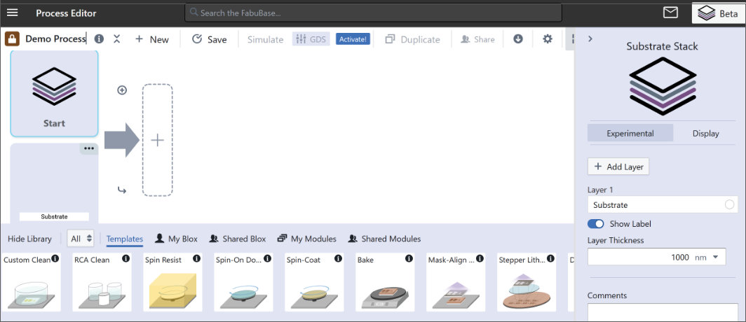
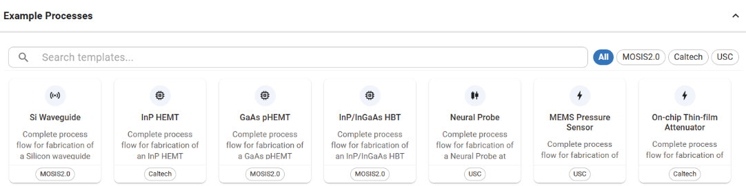
Fab Service Explorer
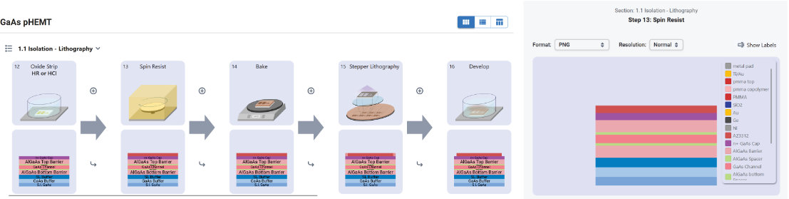
The Fab Service Explorer enables you to interact with available fabrication capabilities, process flows, and device structures available through MOSIS 2.0 prototyping and fabrication services.
Browse technology process flows available through MOSIS 2.0 and our nanofabrication facility partners.
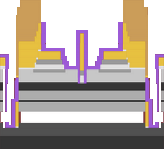
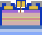
See process steps alongside fabricated device schematics provides additional information on materials used.
Use the FabuBlox Process Design UI to create your own custom flow and submit to MOSIS 2.0 engineers for evaluation and feedback.