Offered MPW Services - Si CMOS, Compound Semiconductor
MOSIS 2.0 offers a comprehensive range of Multi-Project Wafer (MPW) services, supporting both silicon CMOS and advanced compound semiconductor technologies. Our platform provides seamless access to a wide array of commercial silicon MPW services from leading foundries, including TSMC, Intel, Samsung, SkyWater Technology, GlobalFoundries, and Tower Semiconductor. Covering technology nodes from 12 nm to 350 nm and supporting wafer sizes from 100mm to 300mm, MOSIS 2.0 enables the development of diverse applications, from state-of-the-art research to mature silicon-based products.
In addition to silicon CMOS technologies, MOSIS 2.0 collaborates with three DoW-volume fabs—HRL Laboratories, Teledyne, and Northrop Grumman—to offer advanced group III/V MPW services, including GaN HEMT, GaAs HEMT, and InP HBT/HEMT technologies. These partnerships provide industry-leading solutions for high-performance RF, power electronics, and photonic applications. Furthermore, our collaboration with WIN Semiconductors adds cutting-edge GaAs and GaN HEMT MPW services, supporting technology nodes from 100 nm to 500 nm, which are ideal for wireless communication and high-frequency electronic devices.
With comprehensive front-end and back-end capabilities, full customization options, and support for heterogeneous integration, MOSIS 2.0 provides a versatile and robust platform to meet the diverse needs of our customers. We are also actively collaborating with CA DREAMS hub members, other Microelectronics Commons superhubs, and CHES partners, which offer additional resources and expertise to further enhance our MPW services. Our extensive MPW services, combined with comprehensive chip design support, enable innovators to realize their cutting-edge semiconductor products with efficiency and confidence.
MPW Partners

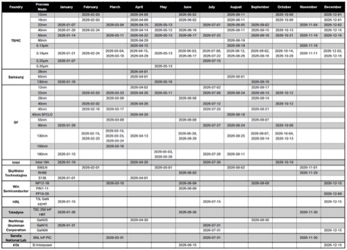
Tapeout Schedule
Don't miss out on any upcoming MOSIS 2.0 MPW runs. Click the button below to sign up and secure your spot!
Please use the fields below to find a tapeout schedule for our available foundry services.
Our DIB partners' MPW schedules are subject to change based on MOSIS 2.0 and Foundry internal schedules. Additional MPW tape-out opportunities may be available upon request for dedicated MPW services, offering customized scheduling and allocation.
Technology Offerings
| Fab Partner | Process Offering | Technology Node | Tapeout Frequency | Wafer Size | |
|---|---|---|---|---|---|
| TSMC | MPW Dedicated | Si CMOS | 12nm, 16nm, 22nm, 28nm, 40nm, 55nm, 65nm, 90nm, 130nm | 2-10 per year | 300mm |
| 180nm, 250nm, 350nm | 2-26 per year | 200mm | |||
| Samsung Foundry | MPW Dedicated | Si CMOS | 28nm, 65nm, 130nm | 2-4 per year | 300mm |
| SkyWater Technology | MPW Dedicated | Si CMOS | 90nm, 130nm | 2-4 per year | 200mm |
| WIN Semiconductors | MPW Dedicated | GaAs pHEMT | 100nm, 150nm, 180nm, 250nm, 450nm, 500nm | 2-4 per year | 150mm |
| GaAs HBT | 4th Gen, 5th Gen, 7th Gen | 2-4 per year | 150mm | ||
| GaN HEMT | 120nm, 150nm, 250nm, 450nm | 2-4 per year | 100mm | ||
| HRL Laboratories | MPW | T3L GaN HEMT | 40nm | 2 per year | 100mm |
| Teledyne | MPW | TSC250 InP HBT | 250nm | 3 per year | 100mm |
| Northrop Grumman | MPW Dedicated | GaN GaN20_PWR HEMT | 90nm, 150nm, 200nm | 4 per year | 100mm |
| MPW | GaAs P3H, P3K6, InP N60E, TF5 | 2-4 per year | 100mm | ||
| Sandia National Lab | MPW | InP PIC | 100nm | 2-4 per year | 100mm |
| RTX Corporation | MPW | Silicon Interposer | 2 per year | 200mm | |
| GlobalFoundries | MPW Dedicated | FDX™ 22FDSOI | multiple | 300mm | |
| Silicon Photonics: GF Fotonix 45 SPCLO (Photonics + Analog + RF) | 2 per year | 300mm | |||
| RFSOI: 45nm, 65-90nm | 2-4 per year | 300mm | |||
| BCD and BCDLite: 55nm, 130nm, 180nm | 200mm | ||||
| Bulk CMOS: 28nm, 40-90nm, 130nm, 180nm | 300mm | ||||
| FinFET 12 LP+ | 300mm | ||||
| GaN: 130nm GaN, 180nm HVGaN | 200mm | ||||
| SiGe BiCMOS: 130nm, 90nm, 45RFSOI, 22nm | 200mm | ||||
| MIM/MOM capacitors/ NVM (MRAM, RRAM) | 200-300mm | ||||
| Intel Foundry | MPW Dedicated | Intel 18A | 4 per year | 300mm | |
Receive notifications for new MOSIS 2.0 offerings and upcoming MPW runs.