Rehan Kapadia
Director MOSIS 2.0
| Foundry Service | Technology Node | Tapeout Date |
|---|---|---|
| Samsung | 65 nm | 8/1/2026 |
Rapid prototyping and process development capability through access to seven university nanofabrication facilities and other experimental prototyping facilities within the Southern California area and throughout the nation.
Supporting both silicon CMOS and advanced compound semiconductor technologies with seamless access to a wide array of commercial silicon MPW services from leading large, medium, and small-volume foundries.
Providing comprehensive chip design services that simplify and streamline the development process, enabling customers to bring their innovative ideas from concept to silicon.
The SWAP Hub provides a suite of test and modeling services to evaluate materials, devices, packages, and full systems across a wide range of environments for mission-critical applications.
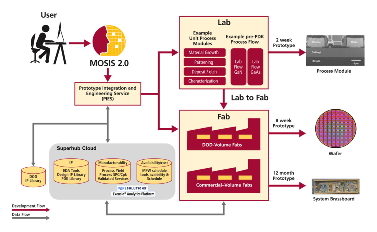
MOSIS 2.0 is the central storefront and gateway to access cutting-edge prototyping services, targeting advanced RF, 5G/6G, and EW applications.
The Prototype Integration and Engineering Service (PIES) Team is at the core of MOSIS 2.0 - a dedicated fab-knowledgeable engineering group that supports designers to accelerate their innovations to solutions.
We invite innovators, researchers, and industry partners to engage with MOSIS 2.0-and join us in advancing next-generation microelectronics.
Director MOSIS 2.0
Fabrication Services
Team Lead
Senior Project Manager
MPW Services Team Lead
Receive notifications for new MOSIS 2.0 offerings and upcoming MPW runs.
This value-added partnership enables customers to access the full suite of GF technologies via the MOSIS 2.0 storefront, including cutting-edge FinFET and FDX™ FD-SOI process technologies, helping innovators move advanced chip designs from concept to fabrication.
Founded at the USC Information Sciences Institute and a core component of California DREAMS, MOSIS 2.0 is helping accelerate innovation and strengthen the U.S. microelectronics ecosystem by bringing together leading foundries through a single access point.
We're grateful to GlobalFoundries for partnering with us to expand access to world-class semiconductor manufacturing capabilities.
Learn more: https://lnkd.in/g27-Fc9F
We're grateful to our presenters, Jon Hacker (@[Teledyne Scientific & Imaging](urn:li:organization:1379764)), @[Istvan Rodriguez](urn:li:person:oE52o6Wa_I) ( Raytheon), @[Maxwell Duffy](urn:li:person:dTndPzWm_c) ( Northrop Grumman), and David Fanning (@[HRL Laboratories, LLC](urn:li:organization:24318)), who shared insights into advanced semiconductor technologies and prototyping opportunities.
Our Director, Rehan Kapadia, provided an overview of the MOSIS 2.0 ecosystem, and Kenneth Zick ( USC Information Sciences Institute) demonstrated the MOSIS 2.0 Accelerated Prototyping Platform (MAPP)—a reusable, programmable prototyping environment that eliminates the need to build custom testbeds, interfaces, and integrations from scratch.
We look forward to continuing the conversation with developers and supporting your journey from concept to prototype and beyond.
Learn more about MOSIS 2.0: https://www.mosis2.com/
Register here: https://lnkd.in/gNFnYS6x
Seats are filling quickly — register now:
🔗 https://lnkd.in/gNFnYS6x
🗓️ Wednesday, June 10
⏰ 12:00 PM – 2:00 PM
📍 Thomas M. Menino Convention & Exhibition Center | Room 108
🍽️ Lunch provided
If you're designing the next generation of RF, mmWave, 5G/6G, photonics, or digital CMOS systems, this is a session you won’t want to miss.
Workshop topics include:
🔹 Advanced & Legacy Silicon CMOS — GlobalFoundries, Intel, SkyWater, Samsung, TSMC
🔹 Compound Semiconductors — GaN HEMT, InP HBT, InP PIC, WIN Semiconductors
🔹 Advanced Packaging & Heterogeneous Integration
🔹 Custom Split-Fab Semiconductor Fabrication
🔹 MOSIS Advanced Prototyping Platform (MAPP) for rapid FPGA-ASIC testing
🔹 IC Design Services
And be sure to stop by Booth 24084 during IMS to meet the MOSIS 2.0 team and learn more. Join us to see how MOSIS 2.0 can help accelerate your next breakthrough.
Thanks to everyone who has stopped by Booth 208 to meet the MOSIS 2.0 / California DREAMS team. We’re looking forward to more conversations this afternoon and evening at the Special Session on GaN Foundries, where MOSIS Director Rehan Kapadia will be speaking beginning at 3:30 PM.
https://lnkd.in/gpvufc7S
See you there!